
Necessity for two spark gaps in DER717 15W reference design
Posted by: IPP
on
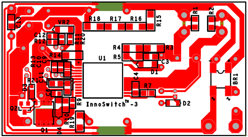
Two sparkgaps have been used in the reference design DER717, one on top and another on the bottom on the same side of the board, both connecting the output terminals to the AC mains. Is it to have increased discharge current rating or to reduce the trace impedance? Could someone brief on the pros and cons in using just one instead of two?
Files
| Attachment | Size |
|---|---|
| DER717_layer_bottom | 112.05 KB |
Comments
Hi Martok,
Thanks for the clarification.
Regards
IPP
Hello IPP,
Multiple Spark Gap
Pros: Suitable for high voltage ESD (>16.5kV) requirement. At high ESD voltage, ESD might happen anywhere from primary to secondary. The best way to redirect high voltage ESD is through adding more spark gap.
Cons: Need more PCB Space.
Single Spark Gap:
Pros: For 15kV-16.5kV ESD voltage only. Needed for compact power supply application.
Cons: Not ok for high voltage ESD requirement