
SCALE-2
Power Integrations’ SCALE™-2 IGBT Gate Drivers use an ASIC chip set specifically-designed to reduce count, save space and increase product reliability and functionality. This approach enables designers to optimize dynamic switching performance and accuracy, delivering design flexibility and reducing time-to-market for applications with IGBT modules ranging from 150 A to 3600 A and 600 V to 6500 V.
The highly-integrated SCALE-2 gate driver chipset implements all required functionality and facilitates easy power scaling up to 60A gate current/ 20W gate power and beyond. The SCALE-2 technology adds new features including secondary-side Intelligent Gate Driver (IGD) ASICs and a primary-side dual channel Logic-to-Driver Interface (LDI) ASIC. In combination with a magnetic coupling a wide range of voltages can be archived. Pre-driver stages are primarily designed to assure optimum performance for direct driving of external n-type DMOS elements by using separate gate resistors for independent control of turn-on and turn-off.
The ASICS are manufactured on an automotive-qualified BiCMOS wafer processing line, ensuring high reliability. Leading analog performance coupled with a reduced digital feature size optimizes the cost/performance ratio.
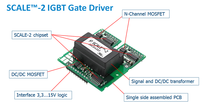
Product example:
Example of SCALE™-2 Schematic
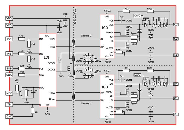
The ASICs: Intelligent Gate Driver (IGD)
A micrograph of a prototype gate driver ASIC is shown in the above figure. Various bonding elements are used to control the specific functionality of different standard products including options for bidirectional-signal-transformer and fiber-optic interfaces. The ASIC also contains a semi-custom array for additional degrees of customization. Advanced control options may be realized through a single programming metal mask. The semi-custom array contains preconfigured cells such as analog comparators, logic gates, primitive devices and pads.
The IGD ASIC provides a regulated +15V gate-emitter voltage for the turn-on and on-state by adjusting the emitter potential at the “Vee” pin (see Fig. 3) with options to set a custom-specific gate-emitter voltage.
The ASIC incorporates circuitry to realize closed-loop control of both the rate of rise [1] and clamping level [2] of the collector-emitter voltage of the IGBT at turn-off. Faster response of the Active Clamping process, reduced turn-off switching losses and enhanced short-circuit turn-off capability can then be achieved.
The ASICS: Logic-to-Driver Interface (LDI)
A micrograph of a Logic-to-Driver Interface ASIC is shown in Fig. 2. The ASIC implements a dual-channel bidirectional transformer interface, a scalable DC/DC converter with dedicated start-up sequence as well as scalable setup and fault management.
SCALE-2 IGBT-drivers couple ASIC technology with a proprietary transformer design enabling the company to provide UL Certification across its entire product range.
A bidirectional transformer interface transmits both command and fault signals via short single pulses to achieve minimum command delay. In case of a signal collision, the fault signal dominates both the command signal and dv/dt induced noise currents by means of a longer pulse duration. The asynchronous fault transfer method also allows the special timing requirements of parallel-connected IGBTs or multi-level converter topologies to be managed, since any fault condition will be apparent at the primary side in less than one microsecond. A preferred fault-management mode reports the fault event in advance of a turn-off of the relevant IGBTs. The delay period before shutdown can be adjusted within the IGD ASIC. For transformer coupled drivers, (see Fig. 3) delays of less than 80ns and ±1ns jitter can be achieved.
Operational Modes
Direct Mode allows both driver channels to be independently driven. This mode offers the highest levels of customer flexibility and is therefore preferred for advanced microcontroller-assisted systems. In half-bridge mode, the ASIC uses only one input as a common command signal and generates two (non-inverted and inverted) outputs. The mode and dead time are adjustable to the needs of the particular application via a single resistor. A third mode is pre-configured to implement interlock or mutual exclusion upon customer request.
Fault Management
On the primary side, any fault state may be stretched by a Blocking Time. During this period, the relevant channel is kept in the off-state. This time is adjustable using a single resistor and can also be set to a minimum of 10µs.
System Integration
SCALE-2 chipset serves as a core technology for implementing the next generation of IGBT driver series. Fig. 4 shows a simplified schematic diagram of a Plug-and-Play IGBT driver for high-voltage IGBT modules up to 6500V with an Advanced Active Clamping function. The driver achieves gate levels of 40A, 6W by using external n-type DMOS elements for both the gate drive and DC/DC converter output stages. The overall component count is reduced by more than 60% compared to the previous SCALE driver chipset and by significantly more when compared to traditional discrete designs.
Nomenclature SCALE-2
